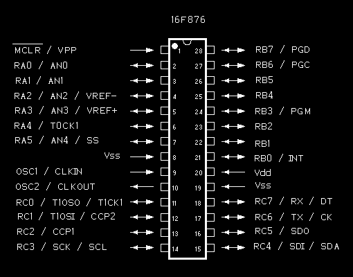
PIC's such as the 16F876 have built-in Analog to Digital Convertor (ADC) hardware. The ADC is connected to the outside world through analog input pins. These pins share functions with other peripherals.
ANALOG
FUNCTIONDIGITAL
FUNCTIONOTHER
FUNCTIONPIN AN0 RA0 2 AN1 RA1 3 AN2 RA2 VREF- 4 AN3 RA3 VREF+ 5 AN4 RA5 SS 7 The above table shows that:
analog pin AN0 is the same pin as digital pin RA0 which is pin 2 on the 16f876,
analog pin AN1 is the same pin as digital pin RA1 which is pin 3 on the 16f876,
analog pin AN4 is the same pin as digital pin RA5 which is pin 7 on the 16f876 etc.The physical location of these pins on the 16f876 is shown on the pin diagram below
16F876 PIN DIAGRAM
To use a pin as an analog input to the ADC, it must be configured to function as an analog inputs to the ADC.
Within XCSB this is done using the ADC_init function.
The following table shows the combination of pins which can be simultaniously assigned the analog input functions on the 16f87x.
config
combinationAN7
RE2AN6
RE1AN5
RE0AN4
RA5AN3
RA3AN2
RA2AN1
RA1AN0
RA00 A A A A A A A A 1 A A A A Vref+ A A A 2 D D D A A A A A 3 D D D A Vref+ A A A 4 D D D D A D A A 5 D D D D Vref+ D A A 6 D D D D D D D D 7 D D D D D D D D 8 A A A A Vref+ Vref- A A 9 D D A A A A A A 10 D D A A Vref+ A A A 11 D D A A Vref+ Vref- A A 12 D D D A Vref+ Vref- A A 13 D D D D Vref+ Vref+ A A 14 D D D D D D D A 15 D D D D Vref+ Vref+ D A NOTE: the 16f876 does not have AN5, AN6 or AN7, however these analog inputs are available on 16f877
This table shows that it is not possible to have the following pin function combination
AN7
RE2AN6
RE1AN5
RE0AN4
RA5AN3
RA3AN2
RA2AN1
RA1AN0
RA0D D D D A D D A
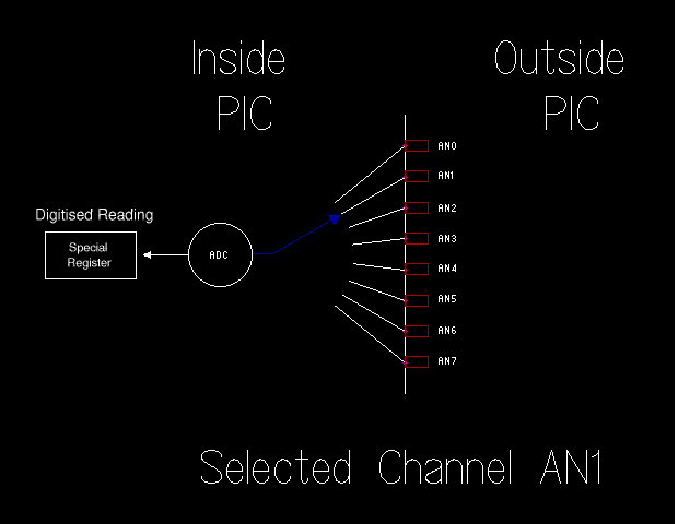
Selecting an analog channel
The ADC hardware is used to read the voltage of a given analog pin. The path between an analog pin and the ADC hardware is refered to as a channel. The channel is refered to by the analog label of the pin used.
The XCSB functions
ADC_read_8bitare told which channel to read from. While the ADC hardware is reading from one channel, that channel is selected and all other analog channels are deselected.
ADC_read_10bitXCSB functions which need to select a channel do so by number. The selected channel is identified on the PIC as pin ANj where j is the channel number and is in the range 0 to 7 (inclusive). (NOTE: channels AN5, AN6 and AN7 are not available on the 16f876)
So:
channel 0 is connected to pin AN0 which is pin 2 on the 16f876,
channel 1 is connected to pin AN1 which is pin 3 on the 16f876,
channel 4 is connected to pin AN4 which is pin 7 on the 16f876
Only pins that have been configured as an analog inputs (using the ADC_init function) can be selected as ADC channels.
ADC Resolution
The resolution of the ADC determins how many units a reading in broken down into.
The PIC ADC is 10 bits wide this means that an analog input can be digtised and read as a value between 0 and 1023. Sometimes dividing an input into 1024 units produces a result which is much too accurate. An example of this would be reading a 16 position switch and dividing this into 1024 units. In this situation we end up with 64 units for switch position 0, 64 units for switch position 1, 64 units for switch position 2 and this repeats with 64 units for each switch position all the way to the last switch position (15). Divding the input into a smaller number of units would be desirable since it reduces the size of the program required to handle the numbers involved and consequently the amount of processing required.
The 10 bit ADC result can be very efficiently converted to an 8 bit result (1024 down to 256). 10 bit values need to be processed as 16 bit words, 8 bit values can be efficiently processed using 8 bit bytes.
The ADC_read_8bit function reads the analog input defined as channel channel_id using the 10 bit ADC, efficiently converts it to an 8 bits value and returns it.